Photobit ble startet i slutten av 1995 av Eric Fossum, en amerikaner hvis eventuelle norske aner er så langt tilbake i tid at han ikke gjør noe stort nummer av det.
Fossum var en fremstående forsker ved NASAs Jet Propulsion Laboratory (JPL), som eies av Caltech. Han forsket på bildedigitalisering. På vegne av NASA søkte de etter metoder for å ta skarpe bilder under dårlige lysforhold og med minimalt batteriforbruk. Det endte med verdens første kamera-på-en-chip, som det ble tatt patent på.
JPL ønsket at kunnskapen skulle komme den kommersielle delen av verden til gode. Derfor lot de Fossum ta med seg patentene for å starte egen virksomhet. De første resultatene finnes allerede i kommersielle produkter på markedet i dag.
Photobit Corporation er 70 mann stort nå, og har skaffet seg salgskontorer i ikke mindre enn 132 land.
Når selskapet, som utvikler og markedsfører teknologi i verdenseliten, nå skal etablere seg utenfor USA, har de plukket ut dr. Johannes Sølhusvik til å bygge opp deres europeiske forsknings- og utviklingsavdeling.
Og avdelingen skal ligge i Oslo.
Her er pressemeldingen Photobit sendte ut tirsdag kveld
Photobit Corporation Opens Research and Development Center in Norway
U.S. Ambassador to Host Reception for Maker of Patented CMOS Image Sensors
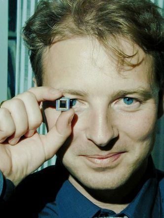
Oslo, Norway—September 21, 1999—Pasadena, California-based Photobit Corporation, the leading supplier of CMOS image sensors, today announced the opening of a European research and development branch in Norway. Photobit made the announcement at Oslo City Hall during a news conference that included a demonstration of the company’s patented CMOS “camera-on-a-chip,” a technology that is considered a breakthrough in digital imaging. Photobit sensors can be used in a wide range of devices, including Internet cameras, digital still cameras, and video cell phones, as well as in machine vision and medical, industrial, and military applications.
On Wednesday, September 22, Photobit will hold an invitation-only open house at the new facility, which is located in the Oslo Research Park. This will be followed by a U.S. embassy reception hosted by the U.S. Ambassador to Norway, David B. Hermelin.
The center will develop CMOS image sensors based on Photobit’s “active-pixel” technology, which has received seven patents and is considered a breakthrough in digital imaging. Key benefits of the technology are: lower power consumption than CCD sensors; on-chip integration of camera functions (hence the term camera-on-a-chip); high image quality; and the ability to manufacture on the same (CMOS) platforms as virtually all microprocessors and memory chips. The latest Photobit offering, the PB-1024, is the world’s fastest megapixel CMOS image sensor. It is capable of capturing more than 500 frames per second, for such applications as motion analysis and machine vision.
“Europe is a hotbed of innovation in the imaging field,” said Dr. Eric R. Fossum, Chief Scientist and Chairman of Photobit Corporation. “By opening a center in Oslo, we are better able to avail ourselves of the high-caliber Scandinavian technological talent in this region and to serve our existing and future OEM customers in Europe and around the world.”
“Locating in Oslo will be a boon to Photobit’s existing and future European customers and partners,” said Dr. Johannes Solhusvik, Manager, Photobit’s Norway office. “Our new proximity will enable us to work more closely with OEMs during product development, thereby better securing their satisfaction and anticipating their needs.”
“The Oslo Research Park is in the heart of Norway’s research and development community,” Dr. Solhusvik added. “More than one-third of the country’s R&D expenditures occur here. Scandinavia’s largest university, the University of Oslo—known for numerous Nobel Prize winners and as the birthplace of object-oriented programming—will be our close neighbor, and we expect to work with the university’s National Microelectronic and Intermedia centers, where next-generation Internet technology is being developed.”
Recent Photobit News
Photobit Corporation, which holds the broad patent for the “CMOS Active-Pixel Sensor Type Imaging System on a Chip,” has since fall 1998 launched a progression of off-the-shelf sensors to commercialize this technology. New chips include: the CIF-size PB-0100, for Internet cameras and video cellular phones; the VGA-format PB-0300, for high-end Internet cameras and small-format digital still photography; the PB-0720, the first CMOS image sensor to conform to the 720 P60 high-definition television standard; and the 500 frames-per-second megapixel PB-1024, which is the world’s fastest CMOS image sensor. In April, Photobit’s founders were recognized for their efforts when the U.S. Space Foundation inducted them, together with Photobit’s core technology, into the Space Technology Hall of Fame.
CMOS’ Advantages Over CCDs
Charge-coupled devices, or CCDs, were the prevailing technology in image capture for thirty (30) years. By the late 1990s, however, they began to be replaced in key applications by CMOS (complementary metal-oxide semiconductor) image sensors. There were several reasons for the shift. First, CMOS sensors draw much less power than CCDs. This allows end products to run longer on batteries, which is a major advantage in hand-held applications such as personal data assistants (PDAs) and video cell phones. Second, CMOS sensors use the same manufacturing platform as most microprocessors and memory chips, making them easier to produce and more cost-effective. Third, by combining all camera functions on-chip-from the capture of photons to the output of digital bits-CMOS image sensors reduce the part count in end products, which in turn enhances reliability, facilitates miniaturization, and allows on-chip programming of frame size, windowing, exposure, and other camera parameters.
- Vi hadde en internasjonal pressekonferanse i Oslo Rådhus tirsdag ettermiddag og kveld, sier Sølhusvik til digi.no.
- Representanter for Financial Times, CNN og annen internasjonal presse var til stede.
Han sier at bakgrunnen for dette valget først og fremst var tilgangen på kompetanse. - Det finnes dyktige folk på dette feltet i Norge, og med et så spennende prosjekt tror jeg ikke det skal by på vanskeligheter å rekruttere dem heller.

Han har allerede rekruttert inn tre kolleger, alle med dyptpløyende tekniske kunnskaper på feltet. De tre er Geir Strand, Steinar Iversen og Marius Evensen.
- Jeg regner med at vi er 30-40 mann om fem år, sier forskningssjefen.
Han sier også at han vil satse på et nært samarbeid med universitets- og forskningsmiljøene. Disse vil til gjengjeld få tilgang på den patenterte kunnskapen Photobit sitter på.
- Vi vil fokusere på utvikling av digital sensorteknologi innen områder som videokonferanse, telemedisin, mobiltelefoni, Internett og intelligente synssystemer. Selv om de største kundene befinner seg utenfor Norges grenser vil utviklingen på sensorteknologi for det europeiske markedet skje i Norge, noe som representerer en mulighet for industriell vekst, sier Sølhusvik.